| CPC H01Q 1/2283 (2013.01) [H01Q 1/40 (2013.01); H01Q 1/48 (2013.01); H01Q 9/0407 (2013.01)] | 20 Claims |
|
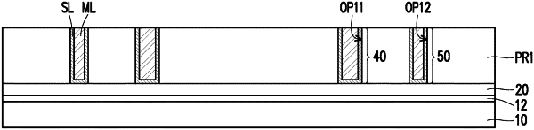
1. A semiconductor package, comprising:
a semiconductor die;
an encapsulation layer, laterally encapsulating the semiconductor die; and
at least one antenna structure, embedded in the encapsulation layer aside the semiconductor die, wherein the at least one antenna structure comprises a dielectric bulk, and a dielectric constant of the dielectric bulk is higher than a dielectric constant of the encapsulation layer,
wherein a top surface of the semiconductor die, a top surface of the encapsulation layer and a top surface of the at least one antenna structure are flushed with each other.
|