| CPC H01Q 1/2283 (2013.01) [H01L 23/49816 (2013.01); H01L 23/49827 (2013.01); H01L 23/5384 (2013.01); H01L 23/5389 (2013.01); H01L 23/66 (2013.01); H01L 24/16 (2013.01); H01L 24/20 (2013.01); H01L 2223/6616 (2013.01); H01L 2223/6677 (2013.01); H01L 2224/04105 (2013.01); H01L 2224/12105 (2013.01); H01L 2224/13144 (2013.01); H01L 2224/13147 (2013.01); H01L 2224/16141 (2013.01); H01L 2224/16227 (2013.01); H01L 2224/16235 (2013.01); H01L 2224/48227 (2013.01); H01L 2225/1023 (2013.01); H01L 2225/1035 (2013.01); H01L 2225/1058 (2013.01); H01L 2924/1421 (2013.01); H01L 2924/15192 (2013.01); H01L 2924/15311 (2013.01); H01L 2924/15321 (2013.01); H01L 2924/19042 (2013.01); H01L 2924/19106 (2013.01)] | 14 Claims |
|
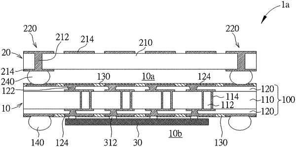
1. A semiconductor package, comprising:
a bottom chip package having a first side and a second side opposing the first side, the bottom chip package comprising a package substrate having a core with at least one plated through-hole, and at least one build-up layer;
a semiconductor chip on the first side or the second side of the bottom chip package;
a discrete antenna device mounted on the first side of the bottom chip package and having a first radiative antenna element; and
conductive elements between the discrete antenna device and the bottom chip package to electrically interconnect the bottom chip package and the discrete antenna device.
|