| CPC H01L 31/1075 (2013.01) [G01S 7/4816 (2013.01); G01S 7/4817 (2013.01); G01S 17/931 (2020.01); H01L 27/14643 (2013.01); H01L 27/14647 (2013.01); H01L 31/028 (2013.01); H01L 31/02027 (2013.01); H01L 31/022466 (2013.01); H01L 31/032 (2013.01); H01L 31/03529 (2013.01); H01L 31/035209 (2013.01); H01L 31/035281 (2013.01); H01L 31/1013 (2013.01); H01S 5/0687 (2013.01); H10K 39/32 (2023.02); G05D 1/024 (2013.01); G05D 2201/0213 (2013.01); H01L 31/0296 (2013.01); H01L 31/0304 (2013.01); H01L 31/0312 (2013.01); H01L 31/0324 (2013.01); H01L 31/035218 (2013.01); H01L 2031/0344 (2013.01)] | 18 Claims |
|
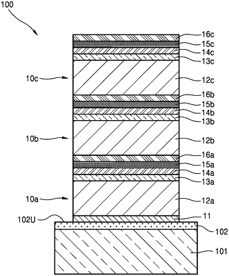
1. A photodetector, comprising:
a first electrode;
a collector layer on the first electrode;
a tunnel barrier layer on the collector layer;
a graphene layer on the tunnel barrier layer;
an emitter layer on the graphene layer; and
a second electrode on the emitter layer,
wherein the collector layer includes a first semiconductor material and the emitter layer includes a second semiconductor material,
wherein at least one semiconductor material of the first semiconductor material and the second semiconductor material includes a transition metal dichalcogenide that is a compound of a transition metal and a chalcogen element that is one of S, Se, or Te,
wherein the emitter layer has a thickness of about 0.3 nm to about 1 μm such that the emitter layer absorbs light and moves electrons and holes, and
wherein the tunnel barrier layer has a thickness of about 0.3 nm to about 1 μm.
|