| CPC H01L 29/7825 (2013.01) [H01L 21/76 (2013.01); H01L 21/762 (2013.01); H01L 29/0653 (2013.01); H01L 29/42368 (2013.01); H01L 29/42376 (2013.01); H01L 29/66704 (2013.01); H01L 29/7835 (2013.01)] | 20 Claims |

|
1. A semiconductor structure, comprising:
a substrate;
an isolation region in the substrate, wherein a top surface of the isolation region level with a top surface of the substrate;
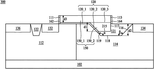
a gate electrode over the substrate and further downwardly extends into the substrate, wherein a portion of the gate electrode below the top surface of the substrate abuts the isolation region;
a gate dielectric layer between the top surface of the substrate and a portion of the gate electrode not extended into the substrate, and the gate dielectric layer further downwardly extending into the substrate between the substrate and the portion of the gate electrode below the top surface of the substrate, and the gate dielectric extending to a bottom of the portion of the gate electrode below the top surface of the substrate without extending along the bottom, wherein an intersection of a portion of the gate dielectric layer above the top surface of the substrate and a portion of the gate dielectric layer below the top surface of the substrate is greater than about 90 degrees and less than about 180 degrees, and the gate dielectric layer had a surface, which is perpendicular to the top surface of the substrate, extending from an end of the bottom of the portion of the gate electrode below the top surface of the substrate to a top surface of the substrate along an angled direction; and
a source region and a drain region formed in the substrate at opposite sides of the gate electrode;
wherein a sidewall of the portion of the gate electrode above the top surface of the substrate and a sidewall of the portion of the gate electrode below the top surface of the substrate form a continuous straight line in a cross-sectional view, and the portion of the gate electrode below the top surface of the substrate has a right-angled trapezoidal profile in a cross-sectional view, and the bottom of the portion of the gate electrode below the top surface of the substrate is parallel to the top surface of the substrate, and an angle formed by an intersection of a sidewall and a bottom surface of the isolation region is greater than about 90 degrees and less than about 180 degrees.
|