| CPC H01L 29/7787 (2013.01) [H01L 21/0217 (2013.01); H01L 21/32136 (2013.01); H01L 23/291 (2013.01); H01L 23/3171 (2013.01); H01L 23/3192 (2013.01); H01L 29/2003 (2013.01); H01L 29/205 (2013.01); H01L 29/404 (2013.01); H01L 29/41758 (2013.01); H01L 29/41775 (2013.01); H01L 29/517 (2013.01); H01L 29/66462 (2013.01); H01L 29/7786 (2013.01)] | 13 Claims |
|
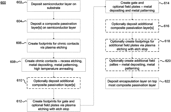
1. A method of fabricating a transistor comprising:
depositing a gate dielectric;
depositing a first passivation layer and a first insulation layer to form a first composite passivation layer, wherein the first passivation layer is disposed between the gate dielectric and the first insulation layer;
forming a gate electrode;
depositing a second passivation layer and a second insulation layer to form a second composite passivation layer, wherein the second passivation layer is disposed between the first insulation layer and the second insulation layer;
forming a first gate field plate disposed between the first insulation layer and the second passivation layer; and
plasma etching at least part of the first composite passivation layer and the second composite passivation layer prior to forming a second gate field plate.
|