| CPC H01L 29/42392 (2013.01) [H01L 21/02359 (2013.01); H01L 29/401 (2013.01); H01L 29/66545 (2013.01); H01L 29/7851 (2013.01); H01L 29/78696 (2013.01)] | 20 Claims |
|
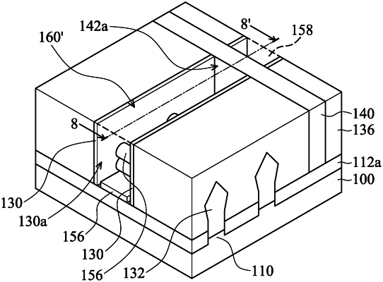
1. A semiconductor device structure, comprising:
a gate electrode layer formed over a semiconductor substrate;
a gate dielectric layer formed between the gate electrode layer and the semiconductor substrate; and
a first gate spacer having a hydrophobic surface that covers a first sidewall of the gate electrode layer, wherein the first sidewall of the gate electrode layer extends along a first sidewall of the gate dielectric layer, so that the first sidewall of the gate dielectric layer is separated from the hydrophobic surface of the first gate spacer.
|