US 11,721,733 B2
Memory transistor with multiple charge storing layers and a high work function gate electrode
Igor Polishchuk, Fremont, CA (US); Sagy Charel Levy, Zichron Yaakov (IL); and Krishnaswamy Ramkumar, San Jose, CA (US)
Assigned to LONGITUDE FLASH MEMORY SOLUTIONS LTD., Dublin (IE)
Filed by LONGITUDE FLASH MEMORY SOLUTIONS LTD., Dublin (IE)
Filed on Jul. 2, 2021, as Appl. No. 17/366,934.
Application 13/288,919 is a division of application No. 12/152,518, filed on May 13, 2008, granted, now 8,063,434, issued on Nov. 22, 2011.
Application 17/366,934 is a continuation of application No. 16/600,768, filed on Oct. 14, 2019, granted, now 11,056,565.
Application 16/600,768 is a continuation of application No. 15/376,282, filed on Dec. 12, 2016, granted, now 10,446,656, issued on Oct. 15, 2019.
Application 15/376,282 is a continuation of application No. 15/335,180, filed on Oct. 26, 2016, granted, now 9,929,240, issued on Mar. 27, 2018.
Application 15/335,180 is a continuation of application No. 14/811,346, filed on Jul. 28, 2015, granted, now 9,502,543, issued on Nov. 22, 2016.
Application 14/811,346 is a continuation of application No. 14/159,315, filed on Jan. 20, 2014, granted, now 9,093,318, issued on Jul. 28, 2015.
Application 14/159,315 is a continuation in part of application No. 13/539,466, filed on Jul. 1, 2012, granted, now 8,633,537, issued on Jan. 21, 2014.
Application 13/539,466 is a continuation in part of application No. 13/288,919, filed on Nov. 3, 2011, granted, now 8,859,374, issued on Oct. 14, 2014.
Claims priority of provisional application 60/940,160, filed on May 25, 2007.
Prior Publication US 2022/0005929 A1, Jan. 6, 2022
This patent is subject to a terminal disclaimer.
Int. Cl. H01L 21/28 (2006.01); H01L 29/423 (2006.01); G11C 16/04 (2006.01); H01L 29/792 (2006.01); H01L 29/51 (2006.01); H01L 29/66 (2006.01); B82Y 10/00 (2011.01); H10B 41/40 (2023.01); H10B 43/00 (2023.01); H10B 43/30 (2023.01); H10B 43/40 (2023.01); H10B 43/50 (2023.01); H01L 29/49 (2006.01); H01L 21/02 (2006.01); H01L 29/06 (2006.01)
CPC H01L 29/4234 (2013.01) [B82Y 10/00 (2013.01); G11C 16/0466 (2013.01); H01L 21/0214 (2013.01); H01L 21/02532 (2013.01); H01L 21/02595 (2013.01); H01L 29/0649 (2013.01); H01L 29/0676 (2013.01); H01L 29/40117 (2019.08); H01L 29/42344 (2013.01); H01L 29/4916 (2013.01); H01L 29/511 (2013.01); H01L 29/512 (2013.01); H01L 29/513 (2013.01); H01L 29/518 (2013.01); H01L 29/66795 (2013.01); H01L 29/66833 (2013.01); H01L 29/792 (2013.01); H01L 29/7926 (2013.01); H10B 41/40 (2023.02); H10B 43/00 (2023.02); H10B 43/30 (2023.02); H10B 43/40 (2023.02); H10B 43/50 (2023.02)] 10 Claims
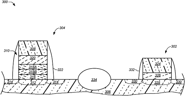
OG exemplary drawing
 
1. A semiconductor memory device comprising:
a semiconductor substrate;
an oxide-nitride-oxide structure formed over the substrate, the oxide-nitride-oxide structure having a tunnel oxide layer, a blocking oxide layer and a multi-layer charge storing layer formed between the tunnel oxide layer and the blocking oxide layer;
the multi-layer charge storing layer including a first layer and a second layer, the first layer being an oxygen-rich oxynitride layer and the second layer being an oxygen-lean oxynitride layer; and
a gate coupled to the oxide-nitride-oxide structure.