| CPC H01L 27/124 (2013.01) [G02F 1/136222 (2021.01); G02F 1/136295 (2021.01); H01L 27/1262 (2013.01)] | 20 Claims |
|
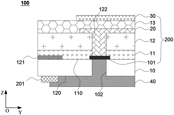
1. An array substrate, comprising:
a base substrate having a first surface and a second surface opposite to the first surface;
a stacked structure disposed on the first surface of the substrate, the stacked structure comprising:
a contact pad disposed on the first surface of the base substrate, wherein the base substrate defines a first via hole at a position corresponding to the contact pad, the first via hole penetrating the first surface and the second surface of the base substrate;
a common-electrode layer connected with the contact pad; and
a gate line isolated from the common-electrode layer and the contact pad;
a common-electrode line disposed on the second surface of the base substrate, wherein an orthographic projection of the gate line on a plane where the common-electrode line is located at least partially overlaps with the common-electrode line; and
a conductive structure connected with the contact pad, and connected to the common-electrode line through the first via hole.
|