| CPC H01L 27/11807 (2013.01) [H01L 23/5226 (2013.01); H01L 27/0207 (2013.01); H01L 23/53233 (2013.01); H01L 23/53238 (2013.01); H01L 23/53266 (2013.01); H01L 2027/11812 (2013.01); H01L 2027/11831 (2013.01); H01L 2027/11837 (2013.01); H01L 2027/11875 (2013.01); H01L 2027/11881 (2013.01); H01L 2027/11887 (2013.01); H01L 2027/11888 (2013.01)] | 20 Claims |
|
1. A semiconductor structure, comprising:
a substrate having a first standard cell, a second standard cell, and a third standard cell, wherein the first standard cell includes an inverter that further includes a first gate stack, wherein the second standard cell includes a logic NAND device that further includes a second and third gate stacks, wherein the third standard cell includes a logic NOR device that further includes a fourth and fifth gate stacks, and wherein the first, second, third, fourth and fifth gate stacks are longitudinally oriented in a first direction;
a first dielectric gate stack disposed between the first and second standard cells;
a second dielectric gate stack disposed between the second and third standard cells, wherein the first and the second dielectric gate stacks are dielectric features and are longitudinally oriented in the first direction;
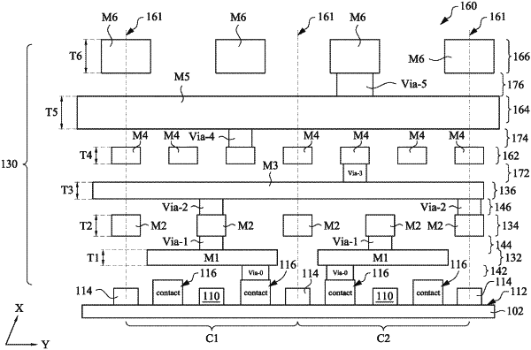
a first metal layer disposed over the first and second dielectric gate stacks, wherein the first metal layer includes a plurality of first metal lines oriented in a second direction being orthogonal to the first direction;
a second metal layer disposed over the first metal layer, wherein the second metal layer includes a plurality of second metal lines oriented in the first direction; and
a third metal layer disposed over the second metal layer, wherein the third metal layer includes a plurality of third metal lines oriented in the second direction,
wherein the first metal lines have a first minimum pitch P1 measured in the first direction,
wherein the second metal lines have a second minimum pitch P2 measured in the second direction,
wherein the third metal lines have a third minimum pitch P3 measured in the first direction, and
wherein the second minimum pitch P2 is greater than the third minimum pitch P3.
|