| CPC H01L 27/0886 (2013.01) [H01L 21/823418 (2013.01); H01L 21/823431 (2013.01); H01L 29/6681 (2013.01); H01L 29/7851 (2013.01); H01L 29/7855 (2013.01)] | 20 Claims |
|
1. A semiconductor structure, comprising:
a substrate;
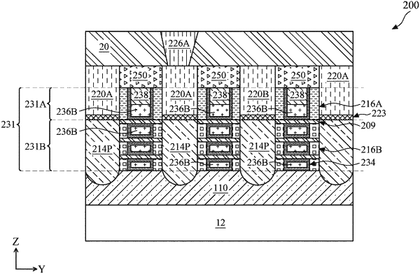
a semiconductor fin protruding from the substrate, wherein the semiconductor fin includes semiconductor layers stacked in a vertical direction;
a gate stack engaging with channel regions of the semiconductor fin, wherein the gate stack includes a first portion disposed over the semiconductor layers and a second portion disposed between the semiconductor layers, wherein the first portion includes a work-function metal (WFM) layer and a metal fill layer disposed over the WFM layer, and wherein the second portion includes the WFM layer but is free of the metal fill layer; and
source/drain (S/D) features disposed adjacent to the gate stack in S/D regions of the semiconductor fin,
wherein the metal fill layer has a first width extending lengthwise between two of the S/D features, the WFM layer has a second width extending lengthwise between the two of the S/D features, and the first and second widths are the same.
|