| CPC H01L 25/0753 (2013.01) [H01L 33/0025 (2013.01); H01L 33/0075 (2013.01); H01L 33/06 (2013.01); H01L 33/24 (2013.01); H01L 33/32 (2013.01); H01L 33/40 (2013.01)] | 14 Claims |
|
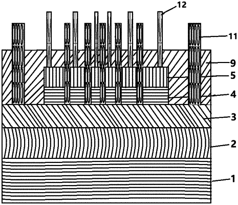
1. A micro-light emitting diode (Micro-LED) array device based on III-nitride semiconductors, structurally comprising from top to bottom in sequence:
a Si substrate;
a GaN buffer layer, wherein the GaN buffer layer is grown on the Si substrate;
an n-type GaN layer, wherein the n-type GaN layer is grown on the GaN buffer layer;
an InGaN/GaN quantum-well active layer, wherein the InGaN/GaN quantum-well active layer is grown on the n-type GaN layer; and
a p-type GaN layer, wherein the p-type GaN layer is grown on the InGaN/GaN quantum-well active layer,
wherein the Micro-LED array device has a plurality of arrayed sector mesa units,
wherein in each arrayed sector mesa unit of the plurality of arrayed sector mesa units, a sector mesa is formed by etching to penetrate through the p-type GaN layer and the InGaN/GaN quantum-well active layer and into the n-type GaN layer,
wherein the Micro-LED array device further comprises a p-type electrode array deposited by evaporation on the p-type GaN layer of the arrayed sector mesa units, and an n-type electrode array deposited by evaporation on the n-type GaN layer of the plurality of arrayed sector mesa units,
wherein n-type electrodes of the n-type electrode array in the each arrayed sector mesa unit surround the sector mesa of the each arrayed sector mesa unit in a form of an annular structure,
wherein the n-type electrodes of the n-type electrode array are blocking walls that are disposed between the sector mesas of the plurality of arrayed sector mesa units and isolate the sector mesas, of the plurality of arrayed sector mesa units, from one another, and
wherein the blocking walls are connected to each other, and each of the blocking walls and the annular structure surrounding the sector mesa of the each arrayed sector mesa unit are connected to each other, and wherein the blocking walls are at least partly disposed at a same height as, and extend above a top of, the InGaN/GaN quantum-well active layer of the sector mesas isolated by the blocking walls.
|