| CPC H01L 24/19 (2013.01) [H01L 21/565 (2013.01); H01L 21/6835 (2013.01); H01L 23/293 (2013.01); H01L 23/3128 (2013.01); H01L 24/13 (2013.01); H01L 24/25 (2013.01); H01L 24/73 (2013.01); H01L 24/96 (2013.01); H01L 25/105 (2013.01); H01L 25/115 (2013.01); H01L 2221/68345 (2013.01); H01L 2221/68368 (2013.01); H01L 2224/13024 (2013.01); H01L 2224/19 (2013.01); H01L 2224/2518 (2013.01); H01L 2224/25171 (2013.01); H01L 2224/73209 (2013.01); H01L 2225/1035 (2013.01); H01L 2225/1058 (2013.01); H01L 2924/3511 (2013.01)] | 20 Claims |
|
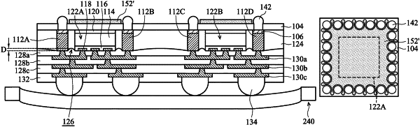
1. A package structure, comprising:
a semiconductor die;
a molding compound layer surrounding the semiconductor die;
a conductive bump over the molding compound layer;
a first polymer-containing layer surrounding and in contact with the conductive bump; and
a second polymer-containing layer disposed over the first polymer-containing layer, wherein a bottom surface of the conductive bump is below a bottom surface of the second polymer-containing layer, wherein a direct projection of the second polymer-containing layer on the first polymer-containing layer is laterally surrounded by outermost edges of the first polymer-containing layer.
|