| CPC H01L 23/66 (2013.01) [H01L 21/4853 (2013.01); H01L 21/4857 (2013.01); H01L 23/4985 (2013.01); H01L 23/49822 (2013.01); H01L 23/49838 (2013.01); H01L 24/16 (2013.01); H01Q 1/38 (2013.01); H01L 2223/6677 (2013.01); H01L 2224/16227 (2013.01)] | 14 Claims |
|
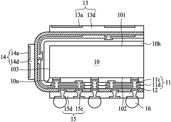
1. A semiconductor device package, comprising:
a first electronic component having an active surface and a first lateral surface;
a first adhesive layer in contact with the active surface and the first lateral surface of the first electronic component; and
a substrate connected to the active surface and the first lateral surface of the first electronic component through the first adhesive layer,
wherein the substrate comprises a first antenna disposed over the first lateral surface of the first electronic component through the first adhesive layer,
wherein the substrate further comprises a first dielectric layer and a second dielectric layer disposed over the first dielectric layer, wherein the second dielectric layer has an opening exposing a bending portion of the first dielectric layer, and wherein the first antenna is disposed over the second dielectric layer.
|