| CPC H01L 23/564 (2013.01) [H01L 21/4853 (2013.01); H01L 21/566 (2013.01); H01L 23/295 (2013.01); H01L 23/3128 (2013.01); H01L 23/49838 (2013.01); H01L 24/16 (2013.01); H01L 2224/16227 (2013.01)] | 20 Claims |
|
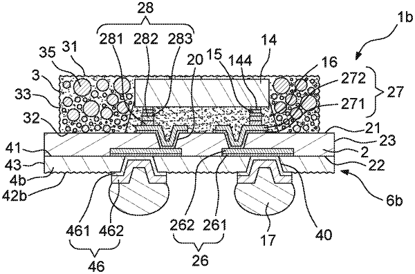
1. A semiconductor package device, comprising:
a semiconductor chip;
an encapsulant encapsulating the semiconductor chip;
a wiring structure disposed on the encapsulant and electrically connected to the semiconductor chip, wherein the wiring structure includes a dielectric layer, and the dielectric layer has a roughened surface; and
an under bump metallization (UBM) on the dielectric layer.
|