| CPC H01L 23/562 (2013.01) [H01L 21/4853 (2013.01); H01L 21/4857 (2013.01); H01L 21/563 (2013.01); H01L 21/565 (2013.01); H01L 21/568 (2013.01); H01L 21/6835 (2013.01); H01L 23/3128 (2013.01); H01L 23/3135 (2013.01); H01L 23/5383 (2013.01); H01L 23/5386 (2013.01); H01L 24/16 (2013.01); H01L 25/0652 (2013.01); H01L 25/0655 (2013.01); H01L 2221/68372 (2013.01); H01L 2224/16227 (2013.01); H01L 2225/06517 (2013.01); H01L 2225/06541 (2013.01); H01L 2225/06586 (2013.01); H01L 2924/18161 (2013.01); H01L 2924/3512 (2013.01)] | 20 Claims |
|
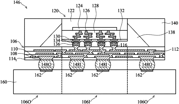
1. A package structure, comprising:
a redistribution structure;
a semiconductor die over the redistribution structure, wherein the semiconductor die has a first sidewall and a second sidewall connected to each other; and
bonding elements below the redistribution structure, comprising
a first row of bonding elements and a second row of bonding elements, wherein the bonding elements in the first row are arranged in a direction parallel to an extending line of the second sidewall, the bonding elements in the second row are arranged in a direction parallel to the extending line of the second sidewall, and in a plan view, the second row of bonding elements is arranged between the first row of bonding elements and the extending line of the second sidewall, wherein a minimum distance between the second row of bonding elements and the first sidewall is greater than a minimum distance between the first row of bonding elements and the first sidewall.
|