US 11,721,598 B2
Method of forming semiconductor device package having testing pads on an upper die
Chen-Hua Yu, Hsinchu (TW); Sung-Feng Yeh, Taipei (TW); Ming-Fa Chen, Taichung (TW); Hsien-Wei Chen, Hsinchu (TW); Hui-Wen Liu, Hsinchu (TW); and Ching-Pin Yuan, Hsinchu (TW)
Assigned to TAIWAN SEMICONDUCTOR MANUFACTURING COMPANY, LTD., Hsinchu (TW)
Filed by Taiwan Semiconductor Manufacturing Company, Ltd., Hsinchu (TW)
Filed on Apr. 18, 2022, as Appl. No. 17/722,935.
Application 16/889,348 is a division of application No. 16/023,504, filed on Jun. 29, 2018, granted, now 10,672,674, issued on Jun. 2, 2020.
Application 17/722,935 is a continuation of application No. 16/889,348, filed on Jun. 1, 2020, granted, now 11,309,223.
Prior Publication US 2022/0238398 A1, Jul. 28, 2022
Int. Cl. H01L 21/56 (2006.01); H01L 21/66 (2006.01); H01L 23/31 (2006.01); H01L 23/544 (2006.01); H01L 23/00 (2006.01); H01L 25/065 (2023.01)
CPC H01L 22/32 (2013.01) [H01L 21/56 (2013.01); H01L 22/22 (2013.01); H01L 22/34 (2013.01); H01L 23/3121 (2013.01); H01L 23/544 (2013.01); H01L 24/09 (2013.01); H01L 24/17 (2013.01); H01L 25/0657 (2013.01); H01L 2223/54426 (2013.01); H01L 2225/06517 (2013.01)] 20 Claims
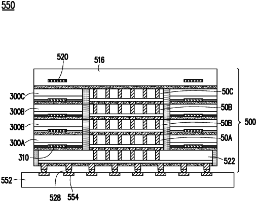
OG exemplary drawing
 
1. A method comprising:
stacking a plurality of first dies on a first carrier substrate to form a device stack;
bonding a second carrier substrate to the device stack;
removing the first carrier substrate from the device stack;
after removing the first carrier substrate, testing the device stack;
after testing the device stack, bonding a second die to the device stack;
singulating the second carrier substrate to form a first device package; and
bonding the first device package to a package substrate.