| CPC H01L 21/823425 (2013.01) [H01L 21/8249 (2013.01); H01L 21/823437 (2013.01); H01L 27/0251 (2013.01); H01L 29/0607 (2013.01); H01L 29/4238 (2013.01); H01L 29/42368 (2013.01); H01L 29/4925 (2013.01); H01L 29/7832 (2013.01); H01L 29/7835 (2013.01); H01L 29/78 (2013.01)] | 17 Claims |
|
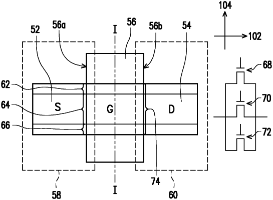
1. A transistor structure, comprising:
a source region and a drain region disposed in a substrate and extend along a first direction;
a polysilicon layer disposed over the substrate and extending along a second direction perpendicular to the first direction, wherein
the polysilicon layer comprises a first edge region, a second edge region, and a channel region between the first edge region and the second edge region, and
the first edge region, the channel region and the second edge region are formed as a gate region between the source region and the drain region in a plane view; and
a gate insulation layer disposed between the polysilicon layer and the substrate, wherein
the transistor structure comprises a first edge transistor, a main channel transistor, and a second edge transistor,
a thickness of the gate insulation layer in the main channel transistor is greater than a thickness of the gate insulation layer in the first edge transistor and a thickness of the gate insulation layer in the second edge transistor,
the first edge transistor, the main channel transistor, and the second edge transistor respectively correspond to the first edge region, the channel region, and the second edge region,
the polysilicon layer comprises a first opening pattern at the first edge region and a second opening pattern at the second edge region, the first opening pattern has a first portion overlapping with the gate region, the second opening pattern has a second portion overlapping with the gate region, and
the transistor structure further comprises:
a first isolation structure connected to a first side of the gate insulation layer; and
a second isolation structure connected to a second side of the gate insulation layer, wherein
the first side and the second side are opposite sides of the gate insulation layer,
the polysilicon layer is located on the gate insulation layer, the first isolation structure, and the second isolation structure, and
the substrate has a channel under the gate insulation layer and between the source region and the drain region in the plane view.
|