| CPC H01L 21/76814 (2013.01) [H01L 21/0273 (2013.01); H01L 21/76816 (2013.01); H01L 21/76835 (2013.01)] | 15 Claims |
|
1. A method for via formation, comprising:
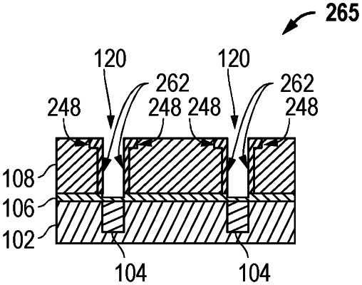
providing a stacked structure on a substrate for a microelectronic workpiece, the stacked structure comprising an organic layer formed over a low-dielectric-constant (low-K) layer;
forming a via through the organic layer to the low-K layer, wherein the forming etches the via into a top portion of the low-K layer;
performing a first ash process to remove a first portion of the organic layer and to leave a second portion of the organic layer, wherein the first ash process causes damage to the top portion of the low-K layer along sidewalls for the via to form a damaged top portion of the low-K layer;
further opening the via through the low-K layer to an underlying layer; and
performing an additional ash process to remove the second portion of the organic layer, wherein the additional ash process causes damage to the low-K layer along sidewalls for the via to form damaged sidewall regions such that the damaged sidewall regions extend in a lateral direction to a lesser extent than the damaged top portions;
performing an etch process, after the additional ash process, that removes the damaged top portions of the low-K layer, wherein the etch process leaves at least a portion of the damaged sidewall regions; and
performing a wet clean process to remove the damaged sidewall regions.
|