| CPC H01L 21/76243 (2013.01) [H01L 21/31155 (2013.01); H01L 21/743 (2013.01); H01L 22/14 (2013.01)] | 17 Claims |
|
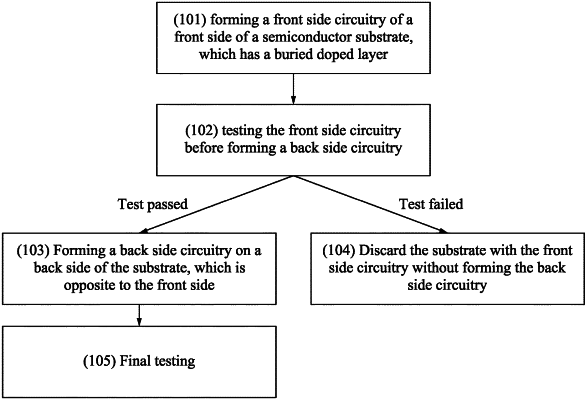
1. A method of making a semiconductor device, comprising:
forming a semiconductor substrate having a buried doped layer within a thickness of the substrate, the substrate having a first surface and a second surface opposite to the first surface, the buried doped layer is at a non-zero depth from the first surface of the substrate, wherein the buried doped layer extends parallel to the first surface of the substrate;
forming a plurality of doped structures within a portion of the semiconductor substrate between the buried doped layer and the first surface of the substrate, wherein each of the plurality of doped structures extends along a vertical direction perpendicular to the first surface of the substrate and is in contact with the buried doped layer;
forming a plurality of transistors over the first surface of the substrate, wherein each of the transistors comprises one or more source/drain structures electrically coupled to the buried doped layer through a corresponding one of the doped structures;
forming a plurality of interconnect structures over the first surface, wherein each of the interconnect structures is electrically coupled to at least one of the transistors; and
testing electrical connections between the interconnect structures and the transistors based on detecting signals present in the buried doped layer through the second surface of the semiconductor substrate.
|