| CPC H01L 21/32136 (2013.01) [H01J 37/32715 (2013.01); H01J 37/32724 (2013.01); H01L 21/0228 (2013.01); H01L 21/02274 (2013.01); H01L 21/3065 (2013.01); H01L 21/30621 (2013.01); H01L 21/31116 (2013.01); H01L 21/31122 (2013.01); H01L 21/32138 (2013.01); H01L 21/67063 (2013.01); H01L 21/67069 (2013.01); H01L 21/67103 (2013.01); H01L 21/67207 (2013.01); H01L 21/67259 (2013.01); H01L 21/6831 (2013.01); H01J 2237/2001 (2013.01); H01J 2237/3341 (2013.01)] | 10 Claims |
|
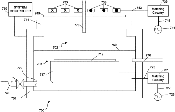
1. An apparatus for processing a substrate, the apparatus comprising:
a process chamber comprising a showerhead and a substrate support for holding the substrate having a material,
a plasma generator, and
a controller having at least one processor and a memory,
wherein the at least one processor and the memory are communicatively connected with one another,
the at least one processor is at least operatively connected with flow-control hardware, and
the memory stores machine-readable instructions for:
causing identification of process conditions for an atomic layer etching process of the material using a modification gas and a removal gas; and
causing performance of the atomic layer etching process on the material on the substrate by:
causing introduction of the modification gas to modify a surface of the material, the modification gas having a modification energy and a desorption energy with respect to the material to be etched, and
causing introduction of the removal gas and generation of a plasma to remove the modified surface,
wherein the modification energy is less than the desorption energy, and the desorption energy is less than a surface binding energy of the material;
wherein the identification of the process conditions comprises causing selection of a substrate temperature for introduction of the modification gas, wherein an ion energy provided by the substrate temperature is between the modification energy and the desorption energy; and
further comprising wherein the material has a surface binding energy greater than about 6 eV, and wherein the machine-readable instructions further comprises causing of setting the substrate at a temperature to provide an ion energy between the modification energy and the desorption energy prior to the causing performance of the atomic layer etching process.
|