| CPC H01L 21/2007 (2013.01) [H01L 21/0226 (2013.01); H01L 21/56 (2013.01); H01L 21/603 (2021.08)] | 16 Claims |
|
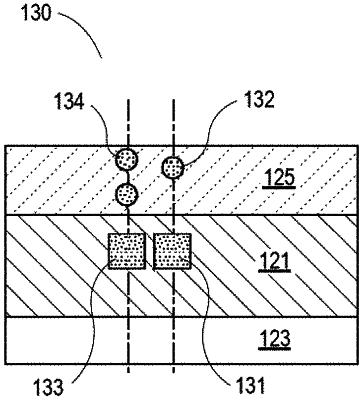
1. An apparatus of bonded wafers, comprising:
a first wafer;
a second wafer bonded to the first wafer; and
a stress compensation layer between the first wafer and the second wafer, and in contact with both the first wafer and the second wafer, wherein:
the first wafer has a first stress level at a first location of the first wafer, and a second stress level at a second location of the first wafer, where the second stress level is different from the first stress level; and
the stress compensation layer includes a first material at a first location of the stress compensation layer overlapping with the first location of the first wafer, a second material at a second location of the stress compensation layer overlapping with the second location of the first wafer, the stress compensation layer induces a third stress level at the first location of the first wafer, and a fourth stress level at the second location of the first wafer, where the third stress level is different from the fourth stress level, and the first material is different from the second material, wherein the stress compensation layer is between the first wafer and the second wafer, and in contact with both the first wafer and the second wafer.
|