| CPC H01L 21/0337 (2013.01) [H10B 12/03 (2023.02); H01L 21/32139 (2013.01)] | 7 Claims |
|
1. A semiconductor device, comprising:
a substrate; and
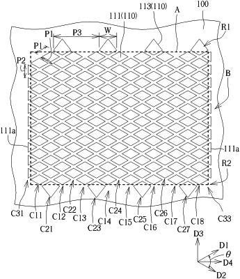
a material layer disposed on the substrate, the material layer comprising a plurality of first patterns, a plurality of second patterns and a plurality of third patterns, the first patterns and the second patterns being parallel and separately arranged in an array arrangement, the second patterns being disposed at two opposite sides of the first patterns, the third patterns being parallel and separately disposed at another two opposite sides of the first patterns, wherein a dimension of each of the third patterns is greater than that of each of the first patterns, and each of the third patterns has a continuously shrunk width which is continuously shrunk along a direction being away from the first patterns.
|