| CPC G11C 29/56012 (2013.01) | 20 Claims |
|
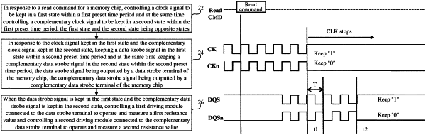
1. A method for testing a memory chip, comprising:
in response to a read command for the memory chip, controlling a clock signal to be kept in a first state within a first preset time period and at the same time controlling a complementary clock signal to be kept in a second state within the first preset time period, the first state and the second state being opposite states;
in response to the clock signal kept in the first state and the complementary clock signal kept in the second state, keeping a data strobe signal in the first state within a second preset time period and at the same time keeping a complementary data strobe signal in the second state within the second preset time period, the data strobe signal being outputted by a data strobe terminal of the memory chip, the complementary data strobe signal being outputted by a complementary data strobe terminal of the memory chip; and
when the data strobe signal is kept in the first state and the complementary data strobe signal is kept in the second state, controlling a first driving module connected to the data strobe terminal to operate and measure a first resistance value and controlling a second driving module connected to the complementary data strobe terminal to operate and measure a second resistance value.
|