US 11,721,376 B2
Memory device, operation method of memory device and operation method of memory circuit
Hung-Li Chiang, Taipei (TW); Chung-Te Lin, Tainan (TW); Shy-Jay Lin, Hsinchu County (TW); Tzu-Chiang Chen, Hsinchu (TW); Ming-Yuan Song, Hsinchu (TW); and Hon-Sum Philip Wong, Stanford, CA (US)
Assigned to Taiwan Semiconductor Manufacturing Company, Ltd., Hsinchu (TW)
Filed by Taiwan Semiconductor Manufacturing Company, Ltd., Hsinchu (TW)
Filed on Apr. 21, 2022, as Appl. No. 17/726,509.
Application 17/726,509 is a continuation of application No. 17/103,914, filed on Nov. 24, 2020, granted, now 11,342,015.
Prior Publication US 2022/0246189 A1, Aug. 4, 2022
Int. Cl. G11C 11/16 (2006.01); G11C 11/18 (2006.01); H10B 61/00 (2023.01)
CPC G11C 11/1659 (2013.01) [G11C 11/1673 (2013.01); G11C 11/1675 (2013.01); G11C 11/18 (2013.01); H10B 61/10 (2023.02)] 20 Claims
OG exemplary drawing
 
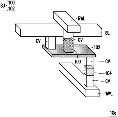
1. A memory device, comprising:
a magnetic tunnel junction (MTJ);
a spin orbit torque (SOT) layer, in contact with a terminal of the MTJ;
a bit line and a write word line, configured to control a first current path across the SOT layer, wherein the bit line is connected to the SOT layer without any switching device in between, and the write word line is selectively connected to the SOT layer through a two-terminal selector; and
a read word line, connected to another terminal of the MTJ without any switching device in between.