|
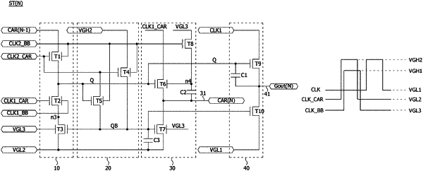
1. A gate driving circuit, comprising: signal transmitters receiving a start pulse, a shift clock, a charge/discharge clock, a back-bias clock, a high-potential driving voltage, and a low-potential reference voltage, and connected in a cascade structure, an Nth (N is a positive integer) signal transmitter of the signal transmitters including: a first control node; a second control node; a first controller controlling charging and discharging of the first control node by using at least one transistor to which the back-bias clock is inputted; a second controller controlling charging and discharging of the second control node; a first output buffer outputting a carry pulse in response to voltages of the first and second control nodes; and a second output buffer outputting a gate pulse; wherein a high voltage of the charge/discharge clock is different from a high voltage of the back-bias clock, and a low voltage of the charge/discharge clock is different from a low voltage of the back-bias clock.
|