| CPC G09G 3/3266 (2013.01) [G09G 3/2096 (2013.01); G11C 19/28 (2013.01); G09G 2310/0286 (2013.01); G09G 2310/08 (2013.01); G09G 2330/028 (2013.01); H10K 59/12 (2023.02)] | 19 Claims |
|
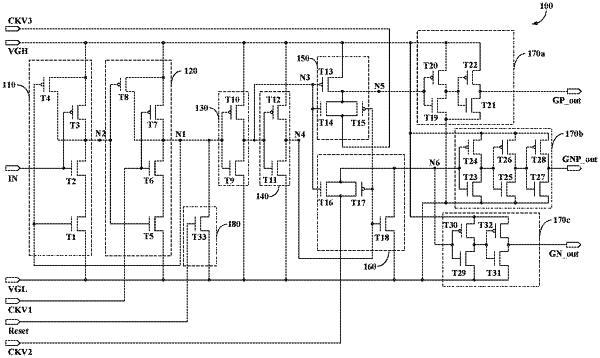
1. A shift register circuit comprising:
an input circuit configured to: in response to at least one of an input terminal providing an input pulse and a first node being at a low potential, bring a second node into conduction with a high-potential voltage terminal providing a high-potential voltage signal, and in response to both the input terminal and the first node being at a high potential, bring the second node into conduction with a low-potential voltage terminal providing a low-potential voltage signal;
a first control circuit configured to: in response to at least one of a first clock signal terminal providing a first clock signal and the second node being at a low potential, bring the first node into conduction with the high-potential voltage terminal, and in response to both the first clock signal terminal and the second node being at a high potential, bring the first node into conduction with the low-potential voltage terminal;
a second control circuit configured to: in response to the first node being at a high potential, bring a third node into conduction with the low-potential voltage terminal, and in response to the first node being at a low potential, bring the third node into conduction with the high-potential voltage terminal;
a third control circuit configured to: in response to the third node being at a high potential, bring a fourth node into conduction with the low-potential voltage terminal, and in response to the third node being at a low potential, bring the fourth node into conduction with the high-potential voltage terminal;
a fourth control circuit configured to: in response to the third node being at low potential and the fourth node being at high potential, bring a fifth node into conduction with the high-potential voltage terminal, and in response to the third node being at high potential and the fourth node being at low potential, bring the fifth node into conduction with a third clock signal terminal providing a third clock signal;
a fifth control circuit configured to: in response to the third node being at a low potential and the fourth node being at a high potential, bring a sixth node into conduction with the low-potential voltage terminal, and in response to the third node being at a high potential and the fourth node being at a low potential, bring the sixth node into conduction with a second clock signal terminal providing a second clock signal;
a first output circuit configured to: in response to the fifth node being at a low potential, bring a first output terminal providing a first output signal into conduction with the low-potential voltage terminal, and in response to the fifth node being at a high potential, bring the first output terminal into conduction with the high-potential voltage terminal;
a second output circuit configured to: in response to the sixth node being at a low potential, bring a second output terminal providing a second output signal into conduction with the high-potential voltage terminal, and in response to the sixth node being at a high potential, bring the second output terminal into conduction with the low-potential voltage terminal; and
a third output circuit configured to: in response to the sixth node being at a low potential, bring a third output terminal providing a third output signal into conduction with the low-potential voltage terminal, and in response to the sixth node point being at a high potential, bring the third output terminal into conduction with the high-potential voltage terminal.
|