| CPC G09G 3/32 (2013.01) [G09G 3/3266 (2013.01); G09G 3/20 (2013.01); G09G 3/325 (2013.01); G09G 2300/0842 (2013.01); G09G 2300/0861 (2013.01); G09G 2310/0286 (2013.01); G09G 2310/061 (2013.01); G09G 2310/08 (2013.01); G09G 2330/021 (2013.01); G09G 2340/0435 (2013.01); G11C 19/28 (2013.01)] | 18 Claims |
|
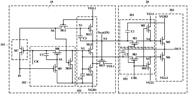
1. A display panel having a driving circuit, comprising:
a driving circuit comprising N stages of cascaded shift registers, wherein N≥2, and each of the N stages of cascaded shift registers comprises: a first control part and a second control part;
wherein the first control part is configured to receive at least an input signal and control a signal of a first node and a signal of a second node in response to at least a first clock signal, and the first control part is configured to receive a first voltage signal and a second voltage signal and control a signal of a third node in response to a signal of the first node and a signal of the second node, wherein the first voltage signal is a high level signal, and the second voltage signal is a low level signal; and the second control part comprises a first control unit, a second control unit, and a third control unit;
the first control unit is configured to receive a third voltage signal and a signal of the third node and control a signal of a fourth node in response to a frequency control signal;
the second control unit is configured to receive a fourth voltage signal and a signal of the second node and control a signal of a fifth node in response to the frequency control signal, wherein one of the third voltage signal or the fourth voltage signal is a high level signal, and the other one of the third voltage signal or the fourth voltage signal is a low level signal; and
the third control unit is configured to receive a fifth voltage signal and generate an output signal in response to a signal of the fourth node; or the third control unit is configured to receive a sixth voltage signal and generate an output signal in response a signal of the fifth node, wherein the fifth voltage signal is a high level signal, and the sixth voltage signal is a low level signal;
wherein a display region of the display panel comprises a first region and a second region, and the frequency control signal comprises a first frequency control signal and a second frequency control signal;
one shift register of the N stages of cascaded shift registers connected to a display unit in the first region is configured to receive the first frequency control signal, and one shift register of the N stages of cascaded shift registers connected to a display unit in the second region is configured to receive the second frequency control signal; and
the first frequency control signal and the second frequency control signal are signals of different potentials during at least part of a preset time period during which the display panel is operating; and
wherein a data refresh frequency of the display unit in the first region is a first frequency F1, and a data refresh frequency of the display unit in the second region is a second frequency F2, wherein F1<F2; and
a time length of the preset time period is T0, wherein 1/F2<T0<1/F1.
|