| CPC G09G 3/2092 (2013.01) [G09G 3/20 (2013.01); G09G 3/3266 (2013.01); G09G 3/3674 (2013.01); G09G 2310/0286 (2013.01); G09G 2310/08 (2013.01); G11C 19/28 (2013.01)] | 19 Claims |
|
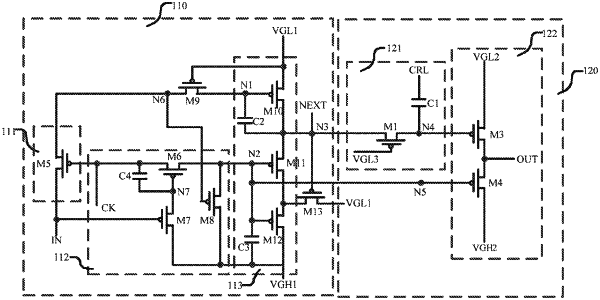
1. A display panel, comprising:
a driver circuit comprising N stages of cascaded shift registers, wherein N≥2, and each of the N stages of cascaded shift registers comprises: a first control part and a second control part;
wherein the first control part is configured to receive at least an input signal and controls a signal of a first node and a signal of a second node in response to at least a first clock signal, and the first control part is configured to receive a first voltage signal and a second voltage signal and controls a signal of a third node in response to a signal of the first node and a signal of the second node, wherein the first voltage signal is a low level signal, and the second voltage signal is a high level signal; and the second control part comprises a first control unit and a second control unit;
the first control unit is configured to receive a signal of a preset node and a first output control signal and control a signal of a fourth node, wherein the preset node is one of the second node or the third node; and
the second control unit is configured to receive a third voltage signal and generate an output signal in response to a signal of the fourth node, or the second control unit is configured to receive a fourth voltage signal and generate an output signal in response to a signal of a fifth node, wherein the fifth node, the second node and the third node are three independent nodes, the fifth node is directly electrically connected to one of the second node or the third node that is not the preset node, the third voltage signal is a low level signal, and the fourth voltage signal is a high level signal;
a first output control signal received by a shift register at an M1-th stage is a signal of the preset node of a shift register at an M2-th stage, wherein 1≤M1≤N, 1≤M2≤N, 1≤|M1−M2|≤i, and 2≤i≤N−1.
|