| CPC G09G 3/20 (2013.01) [G06F 3/044 (2013.01); G06F 3/04166 (2019.05); G09G 2310/0286 (2013.01); G09G 2310/08 (2013.01)] | 17 Claims |
|
1. A display panel, comprising:
a display area, in which a plurality of scanning signal lines are provided; and
a non-display area, in which a shift register circuit is provided,
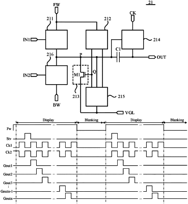
wherein the shift register circuit comprises a plurality of cascaded shift register units, and each of the plurality of shift register units comprises a scanning control terminal, a signal output terminal, a first level signal terminal, a pull-down module and a pull-down control module;
wherein in one of the plurality of shift register units, the pull-down module is electrically connected to a first node, a second node, the first level signal terminal and the signal output terminal separately;
the pull-down module is configured to transmit a first level signal of the first level signal terminal to the second node and the signal output terminal under the control of a potential of the first node; the pull-down module comprises at least a first transistor; a gate of the first transistor is electrically connected to the first node; the pull-down control module is electrically connected to the first node and the scanning control terminal separately; and the pull-down control module is configured to control a scanning control signal of the scanning control terminal to be transmitted to the first node;
wherein in a scanning phase of a frame, the scanning control signal is at an enable level controlling the first transistor to be turned on; in a non-scanning phase of the frame, the scanning control signal comprises a disable level controlling the first transistor to be turned off; and
wherein the signal output terminal of the each of the plurality of shift register units is electrically connected to a respective one of the plurality of scanning signal lines; in the scanning phase, the signal output terminal of the each of the plurality of shift register units sequentially outputs a scanning signal at an enable level; and in the non-scanning phase, the signal output terminal of the each of the plurality of shift register units outputs a scanning signal at a disable level.
|