| CPC G06F 3/0656 (2013.01) [G06F 3/0604 (2013.01); G06F 3/0652 (2013.01); G06F 3/0659 (2013.01); G06F 3/0679 (2013.01); G06F 12/0246 (2013.01); G06F 12/0882 (2013.01); G06F 2212/7201 (2013.01); G06F 2212/7205 (2013.01); G06F 2212/7209 (2013.01)] | 24 Claims |
|
1. A NAND storage device, the NAND storage device comprising:
an array of NAND storage devices;
a controller including:
a memory to hold a buffer; and
processing circuitry to:
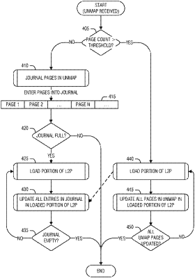
count data portions specified in a delete command, the delete command provided to remove the data portions from a NAND storage device in the array of NAND storage devices; and
write the data portions in the buffer when the count of data portions is below a threshold instead of updating a logical-to-physical mapping of the data portions.
|