| CPC G05F 1/575 (2013.01) [G05F 3/24 (2013.01)] | 13 Claims |
|
1. A system comprising:
a voltage regulator configured to receive a first reference voltage and output a regulated voltage;
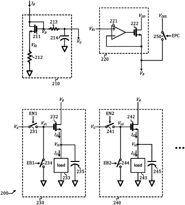
a bias voltage generator comprising a diode-connect transistor and a resistor connected in series configured to receive a bias current and output a reference gate voltage; and
a plurality of switch-load circuits, each of said plurality of switch-load circuits comprising a common-drain transistor configured to receive power from the regulated voltage, receive control from the reference gate voltage via a switch controlled by a logical signal, and output a supply voltage to a load shunt with a decoupling capacitor, wherein a size of the common-drain transistor is scaled from a size of the diode-connect transistor in accordance with a ratio between a current of the load and the bias current, wherein:
the diode-connect transistor and the resistor connected in series establish a bias voltage equal to a threshold voltage of the diode-connect transistor plus an over-drive voltage of the diode-connect transistor plus a product of the bias current and a resistance of the resistor,
the bias voltage reference generator further comprising a low-pass filter configured to filter the bias voltage into the reference gate voltage, and
a length of the common-drain transistor is equal to a length of the diode-connect transistor, a width of the common-drain transistor is equal to a width of the diode-connect transistor times the ratio between the current of the load and the bias current.
|