| CPC G02F 1/163 (2013.01) [G02F 1/155 (2013.01); G02F 1/161 (2013.01); H04N 23/75 (2023.01); G02F 2001/1536 (2013.01)] | 16 Claims |
|
1. An optical panel, comprising:
a first transparent substrate;
a second transparent substrate arranged opposite the first transparent substrate;
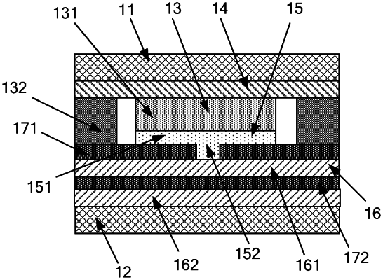
an electrochromic assembly located between the first transparent substrate and the second transparent substrate and including a plurality of electrochromic pixel-units that are arranged in an array, a shielding and spacing wall being arranged between two adjacent of the plurality of electrochromic pixel-units;
a first transparent electrode layer arranged between the electrochromic assembly and the first transparent substrate;
a second transparent electrode layer, arranged between the electrochromic assembly and the second transparent substrate, includes a plurality of pixel electrodes corresponding to the plurality of electrochromic pixel-units, each pixel electrode being arranged on a side surface of a corresponding electrochromic pixel-unit away from the first transparent electrode layer, electrically contacting the electrochromic pixel-unit, and being insulated from the shielding and spacing wall; and
a plurality of transparent electrode wires including first transparent electrode wires located on a first wiring layer and second transparent electrode wires located on a second wiring layer, the first wiring layer is located between the second wiring layer and the electrochromic assembly,
wherein the first transparent electrode layer and the second transparent electrode layer are configured to provide a first driving voltage to the plurality of electrochromic pixel-units and collect a first image with a plurality of image regions by scanning along the plurality of transparent electrode wires as scanning lines, determine brightness levels of each of the plurality of image regions, and provide a second driving voltage causing the light transmittance of the plurality of electrochromic pixel-units to be negatively correlated to the brightness level of the plurality of image regions.
|