| CPC G02F 1/134309 (2013.01) [B60J 3/06 (2013.01); G02F 1/1339 (2013.01); G02F 1/13725 (2013.01); G02F 1/133531 (2021.01); G02F 1/1337 (2013.01); G02F 2202/04 (2013.01)] | 14 Claims |
|
1. An optical device comprising:
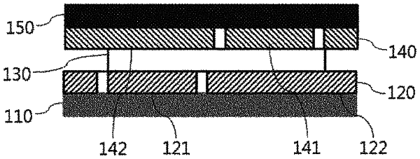
an optical film, wherein the optical film comprises first and second base films disposed to face each other; and a light modulation layer between the first and second base films,
wherein a first electrode layer and a second electrode layer are formed on surfaces of the first and second base films respectively that face each other,
wherein each electrode layer comprises a first region configured to apply an electric field to the light modulation layer, and a second region configured to connect to an external power source to supply power to the first region for applying the electric field,
wherein the first region is a central compartment and the second region is a plurality of peripheral compartments surrounding the central compartment,
wherein at least one peripheral compartment among the plurality of peripheral compartments in the second region is a region A that is electrically connected to the first region via a passage structure, and at least one peripheral compartment among the plurality of peripheral compartments in the second region is a region B that is not electrically connected to the first region,
wherein the region A formed on the first base film and the region A formed on the second base film are disposed so as not to face each other, wherein each electrode layer is scribed to form the regions A and B.
|