| CPC G01N 21/9501 (2013.01) [G01N 21/8851 (2013.01); G06F 30/3323 (2020.01); G06F 30/398 (2020.01); G06T 7/001 (2013.01); H01L 22/12 (2013.01); H01L 22/20 (2013.01); G01N 2021/8861 (2013.01); G01N 2021/8864 (2013.01); G01N 2021/8874 (2013.01); G06T 2207/30148 (2013.01)] | 10 Claims |
|
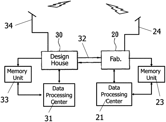
1. A method for performing smart semiconductor wafer defect calibration by means of a data processing apparatus and a storage apparatus, the method comprising:
providing an integrated circuit design layout file, the integrated circuit design layout file has a plurality of circuit layout patterns and is stored into the storage apparatus;
processing a wafer fabrication process, a semiconductor manufacturing fab forms the plurality of circuit layout patterns on the wafer according to the integrated circuit design layout file;
processing a wafer defect scan and inspection by a defect inspection tool to obtain a defect inspection data, the data processing apparatus transforms the defect inspection data into a defect text and image data file and stores into the storage apparatus;
performing a coordinate conversion and coordinate deviation calibration with the integrated circuit design layout file and defect text and image file by the data processing apparatus;
providing a calibration factor by comparing the defect size and defect area in the defect text and image data file with a SEM defect size and SEM defect area for the plurality of the defects, the calibration factor is generated via statistical analysis, wherein the statistical analysis is performed by collecting an original defect size before the defect size calibration and a real defect size after the defect size calibration to build a statistical model, by which a defect size X-axis and Y-axis data for the defect contour will be corrected;
executing a defect size calibration to multiply each of the defect sizes in the defect text and image data file with the calibration factor to get a defect size data, and the defect size data is stored into the storage apparatus after the defect size calibration;
executing an overlapping procedure by the data processing apparatus, the data processing apparatus retrieves sequentially a defect coordinate, a defect size and a defect area of a defect contour from the defect text and image data file, and overlaps the defect size and the defect area onto a coordinate deviation calibration value at a coordinate deviation area of the circuit layout pattern based on the corresponding defect coordinate after executing the coordinate conversion and coordinate deviation calibration;
executing a Critical Area Analysis (CAA) by the data processing apparatus, based on the overlapping of the calibrated defect size and defect area onto the mapped circuit layout pattern, the data processing apparatus uses the CAA to analyze a critical area within the coordinate deviation area for each of the defects, and decides a Killer Defect Index (KDI) value;
judging whether the defect size and defect area are open circuit failure type or short circuit failure type;
classifying each of the defects based on the KDI value of each defect and a defect intensity value of the defect contour by the data processing apparatus, the classification of the defect includes a Dummy pattern defect, a No risk defect or a Killer defect; and
executing a defect sample selection based on defect classification result by the data processing apparatus.
|