| CPC A61M 37/0015 (2013.01) [A61M 2037/003 (2013.01); A61M 2037/0053 (2013.01); A61M 2037/0061 (2013.01); A61M 2207/00 (2013.01)] | 20 Claims |
|
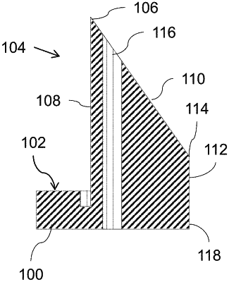
1. A microneedle structure formed from a single crystal of silicon, the microneedle structure comprising:
(a) a substrate having a major surface;
(b) at least one microneedle integrally formed with said substrate so as to project from said major surface, said at least one microneedle comprising:
(i) a penetrating tip formed at an intersection between at least one upright surface perpendicular to said major surface of said substrate and a planar inclined surface corresponding to a (1 1 1) crystallographic plane,
(ii) an expanding portion bounded by a continuation of said at least one upright surface and said inclined surface, and
(iii) a constant cross-section portion bounded by a continuation of said at least one upright surface and a slicing plane extending from an edge of said inclined surface towards, and perpendicular to, said major surface of said substrate,
wherein a width of said inclined surface increases monotonically from said penetrating tip to said edge,
and wherein said slicing plane is also an edge of said substrate.
|