US 11,707,003 B2
Memory device and manufacturing method thereof
Chich-Neng Chang, Pingtung County (TW); Da-Jun Lin, Kaohsiung (TW); Shih-Wei Su, Tainan (TW); Fu-Yu Tsai, Tainan (TW); and Bin-Siang Tsai, Changhua County (TW)
Assigned to UNITED MICROELECTRONICS CORP., Hsinchu (TW)
Filed by United Microelectronics Corp., Hsinchu (TW)
Filed on Jan. 4, 2021, as Appl. No. 17/140,981.
Claims priority of application No. 202011388129.6 (CN), filed on Dec. 1, 2020.
Prior Publication US 2022/0173311 A1, Jun. 2, 2022
Int. Cl. H10N 70/20 (2023.01); H10B 63/00 (2023.01); H10N 70/00 (2023.01)
CPC H10N 70/24 (2023.02) [H10B 63/30 (2023.02); H10N 70/063 (2023.02); H10N 70/826 (2023.02); H10N 70/841 (2023.02)] 13 Claims
OG exemplary drawing
 
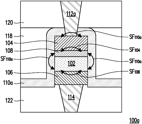
1. A memory device, comprising:
a device substrate;
a bottom electrode, disposed on the device substrate;
a resistance variable layer, disposed on the bottom electrode; and
a top electrode, disposed on the resistance variable layer,
wherein the bottom electrode is formed with a tensile stress, and the top electrode is formed with a compressive stress.