| CPC H10N 70/026 (2023.02) [H10B 63/00 (2023.02); H10B 63/24 (2023.02); H10N 70/231 (2023.02); H10N 70/841 (2023.02); H10N 70/8828 (2023.02)] | 3 Claims |
|
1. A method for manufacturing a phase-change resistive memory including
an upper electrode;
a lower electrode;
an active layer made of an active material;
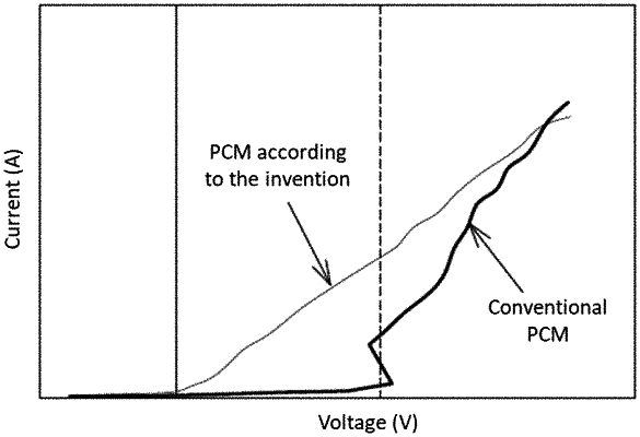
the memory switching from a high resistivity state to a low resistivity state by applying a voltage between the upper electrode and the lower electrode, the material of the active layer being a ternary composed of germanium Ge, tellurium Te and antimony Sb, the ternary including 10% of germanium Ge, 27% of tellurium Te and 63% of antimony Sb, the material of the active layer being in a polycrystalline phase in the high resistivity state and in a crystalline phase in the low resistivity state, the method comprising the steps performed in the following order:
a step of conformably depositing a conducting material layer of the lower electrode onto a substrate;
a step of sputtering using two sputtering targets to form the active layer, a target composed of the element of the chemical formula Ge2Sb2Te5 and a target composed of antimony Sb, and
a step of conformably depositing a conducting material layer of the upper electrode,
wherein the switching from the high resistivity state to the low resistivity state in said memory is obtained by growth of crystals of the polycrystalline phase.
|