US 11,706,996 B2
Magnetoresistive random access memory
Hui-Lin Wang, Taipei (TW); Yu-Ping Wang, Hsinchu (TW); Chen-Yi Weng, New Taipei (TW); Chin-Yang Hsieh, Tainan (TW); Si-Han Tsai, Taichung (TW); Che-Wei Chang, Taichung (TW); and Jing-Yin Jhang, Tainan (TW)
Assigned to UNITED MICROELECTRONICS CORP., Hsin-Chu (TW)
Filed by UNITED MICROELECTRONICS CORP., Hsin-Chu (TW)
Filed on Aug. 31, 2021, as Appl. No. 17/463,541.
Application 17/463,541 is a continuation of application No. 16/589,083, filed on Sep. 30, 2019, granted, now 11,139,428.
Claims priority of application No. 201910827096.1 (CN), filed on Sep. 3, 2019.
Prior Publication US 2021/0399209 A1, Dec. 23, 2021
Int. Cl. H10N 50/80 (2023.01); H10B 61/00 (2023.01); H10N 50/01 (2023.01); H10N 50/85 (2023.01)
CPC H10N 50/80 (2023.02) [H10B 61/00 (2023.02); H10N 50/01 (2023.02); H10N 50/85 (2023.02)] 10 Claims
OG exemplary drawing
 
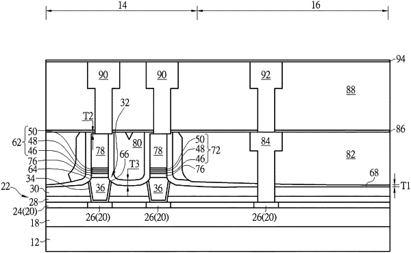
1. A semiconductor device, comprising:
a substrate comprising a magnetic tunneling junction (MTJ) region and a logic region;
a first MTJ on the MTJ region;
a first metal interconnection on the logic region;
a cap layer extending from a sidewall of the first MTJ to a sidewall of the first metal interconnection, wherein the cap layer on the MTJ region and the cap layer on the logic region comprise different thicknesses; and
a second inter-metal dielectric (IMD) layer around the cap layer, wherein top surfaces of the cap layer and the second IMD layer are coplanar.