US 11,706,993 B2
Method of manufacturing magnetoresistive random access memory (MRAM) device
Hui-Lin Wang, Taipei (TW); Tai-Cheng Hou, Tainan (TW); Wei-Xin Gao, Tainan (TW); Fu-Yu Tsai, Tainan (TW); Chin-Yang Hsieh, Tainan (TW); Chen-Yi Weng, New Taipei (TW); Jing-Yin Jhang, Tainan (TW); Bin-Siang Tsai, Changhua County (TW); Kun-Ju Li, Tainan (TW); Chih-Yueh Li, Taipei (TW); Chia-Lin Lu, Taoyuan (TW); Chun-Lung Chen, Tainan (TW); Kun-Yuan Liao, Hsinchu (TW); Yu-Tsung Lai, Tainan (TW); and Wei-Hao Huang, New Taipei (TW)
Assigned to UNITED MICROELECTRONICS CORP., Hsin-Chu (TW)
Filed by UNITED MICROELECTRONICS CORP., Hsin-Chu (TW)
Filed on Dec. 27, 2020, as Appl. No. 17/134,460.
Application 17/134,460 is a division of application No. 16/255,754, filed on Jan. 23, 2019, granted, now 10,916,694.
Claims priority of application No. 201811612412.5 (CN), filed on Dec. 27, 2018.
Prior Publication US 2021/0119115 A1, Apr. 22, 2021
Int. Cl. H01L 43/12 (2006.01); H10N 50/10 (2023.01); H01L 21/768 (2006.01); H01L 21/762 (2006.01); H10N 50/80 (2023.01); H10N 35/01 (2023.01)
CPC H10N 50/10 (2023.02) [H01L 21/762 (2013.01); H01L 21/76802 (2013.01); H10N 50/80 (2023.02); H10N 35/01 (2023.02)] 6 Claims
OG exemplary drawing
 
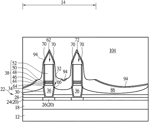
1. A method for fabricating semiconductor device, comprising:
forming a first magnetic tunneling junction (MTJ) on a substrate;
forming a first top electrode on the first MTJ;
forming a first ultra low-k (ULK) dielectric layer on the first MTJ;
performing a first etching process to remove part of the first ULK dielectric layer and form a damaged layer on the first ULK dielectric layer while the first ULK dielectric layer covers the first MTJ and directly contacts a top surface of the first top electrode; and
forming a second ULK dielectric layer on the damaged layer.