| CPC H10K 71/621 (2023.02) [C09K 11/06 (2013.01); G02B 1/18 (2015.01); H10K 30/82 (2023.02); H10K 50/814 (2023.02); H10K 50/824 (2023.02); H10K 50/828 (2023.02); H10K 59/12 (2023.02); H10K 71/166 (2023.02); H10K 30/81 (2023.02); H10K 50/82 (2023.02); H10K 50/822 (2023.02); H10K 59/352 (2023.02); H10K 59/353 (2023.02); H10K 85/324 (2023.02); H10K 2102/3026 (2023.02); H10K 2102/351 (2023.02)] | 46 Claims |
|
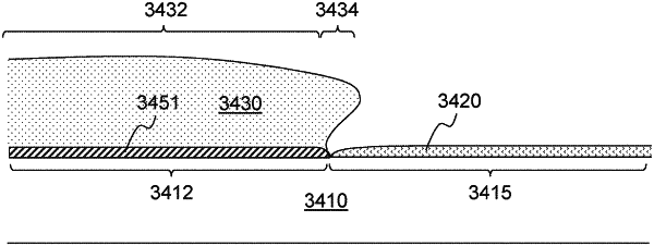
1. A device having a plurality of layers, extending substantially transverse to a lateral aspect of the device, the lateral aspect comprising a first region and a second region, wherein the layers comprise:
a substrate extending across the first region and the second region; and
a conductive coating supported by the substrate and disposed along the second region only;
wherein the conductive coating is formed by actions comprising:
depositing a nucleation inhibiting coating on the substrate along the first region only; and
subjecting the substrate and the nucleation inhibiting coating to a vapor flux of a conductive coating material for which the nucleation inhibiting coating has a low initial sticking probability, so that the conductive coating forms primarily where the substrate is substantially devoid of the nucleation inhibiting coating.
|