| CPC H10K 59/131 (2023.02) [G02F 1/13452 (2013.01); G09G 3/035 (2020.08); G09G 3/3208 (2013.01); H10K 77/111 (2023.02); G09G 2300/0426 (2013.01); G09G 2330/06 (2013.01)] | 15 Claims |
|
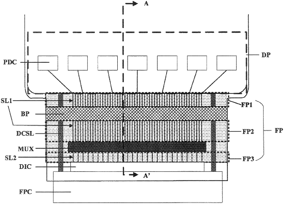
1. A display panel, comprising:
a display part; and
a fanout part;
wherein the display part comprises a plurality of pixel driving circuits;
the fanout part comprises a bendable portion and a multiplexer;
wherein the display panel comprises a plurality of first signal lines extending through the bendable portion, and connecting the plurality of pixel driving circuits to the multiplexer; and
a direct current supply line extending through the bendable portion and electrically connected to the plurality of pixel driving circuits; and
wherein a portion of the direct current supply line is between the multiplexer and the bendable portion and crosses over the plurality of first signal lines;
wherein the fanout part comprises:
a first fanout sub-part abutting the display part;
the bendable portion connected to the first fanout sub-part and spaced apart from the display part by the first fanout sub-part;
a second fanout sub-part connected to the bendable portion and spaced apart from the first fanout sub-part by the bendable portion; and
the multiplexer connected to the second fanout sub-part and spaced apart from the bendable portion by the second fanout sub-part;
wherein the display panel further comprises a driving integrated circuit;
wherein the fanout part further comprises:
a third fanout sub-part connected to the multiplexer and spaced apart from the second fanout sub-part by the multiplexer; and
wherein the display panel comprises a plurality of second signal lines extending through the third fanout sub-part, and connecting the multiplexer to the driving integrated circuit;
wherein the direct current supply line comprises a first portion, a second portion, and a third portion;
the first portion crosses over the plurality of first signal lines;
the second portion extends from the first portion through the bendable portion to electrically connect to the plurality of pixel driving circuits; and
the third portion connects the first portion to a flexible printed circuit;
wherein the display panel further comprises:
a plurality of driving thin film transistor respectively in a plurality of subpixels in the display part; and
a plurality of capacitors respectively in the plurality of subpixels in the display part;
wherein a respective one of the plurality of driving thin film transistors comprises a driving active layer, a driving source electrode, a driving drain electrode, and a driving gate electrode; and
the driving source electrode, the driving drain electrode, the first portion, the second portion, and the third portion are in a same layer and comprise a same material;
wherein a respective one of the plurality of capacitors comprises a first capacitor electrode, a second capacitor electrode, and an insulating layer insulating the first capacitor electrode from the second capacitor electrode;
wherein the plurality of first signal lines comprises a plurality of first type first signal lines and a plurality of second type first signal lines;
orthographic projections of the plurality of first type first signal lines on a base substrate and orthographic projections of the plurality of second type first signal lines on the base substrate are alternately arranged;
the first capacitor electrode, the driving gate electrode, and the plurality of first type first signal lines are in a same layer and comprise a same material; and
the second capacitor electrode, and the plurality of second type first signal lines are in a same layer and comprise a same material.
|