| CPC H10K 59/124 (2023.02) [H04N 23/54 (2023.01); H10K 50/844 (2023.02); H10K 59/126 (2023.02); H10K 59/38 (2023.02)] | 19 Claims |
|
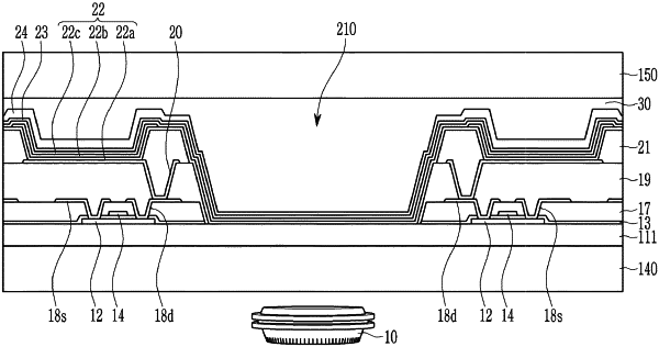
1. A display device comprising:
a display panel comprising a lower substrate and an upper substrate, the display panel forming a light-transmitting area and a display area near the light-transmitting area;
an optical member adjacent to a rear surface of the display panel and overlapping with a portion corresponding to the light-transmitting area; and
at least one of an air layer filled with air comprising nitrogen and a filling layer filled with a silicon-based organic material, the at least one of the air layer and the filling layer being disposed between the upper substrate and the lower substrate,
wherein:
the display area comprises a thin film transistor and an organic light emitting element configured to receive a current from the thin film transistor;
the light-transmitting area does not include a metal layer, which is disposed in the display area; and
the upper substrate and the lower substrate do not have a through-hole structure in the light-transmitting area.
|