| CPC H10K 50/844 (2023.02) [H10K 71/00 (2023.02)] | 20 Claims |
|
1. A method of manufacturing a display device, the method comprising:
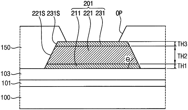
sequentially forming a first conductive layer, a second conductive layer comprising copper (Cu), a third conductive layer, and a fourth conductive layer on a substrate;
patterning each of the first conductive layer, the second conductive layer, the third conductive layer, and the fourth conductive layer to form a conductive pattern including a first layer, a second layer, a third layer, and a fourth layer sequentially on the substrate, after sequentially forming the first to fourth conductive layers;
removing the entire fourth layer of the conductive pattern;
forming a protective layer covering at least a sidewall of the conductive pattern on the substrate; and
forming a display element on the protective layer.
|