| CPC H10K 50/841 (2023.02) [H10K 50/844 (2023.02); H10K 59/122 (2023.02); H10K 59/40 (2023.02); G02F 1/133512 (2013.01); G02F 1/133514 (2013.01); G02F 1/133528 (2013.01); G02F 1/136209 (2013.01); G09G 3/3266 (2013.01); G09G 3/3275 (2013.01); G09G 3/3283 (2013.01); G09G 3/3291 (2013.01); G09G 2300/0408 (2013.01); H01L 27/14678 (2013.01); H10K 50/15 (2023.02); H10K 50/16 (2023.02); H10K 50/17 (2023.02); H10K 50/171 (2023.02); H10K 50/816 (2023.02); H10K 50/828 (2023.02); H10K 59/35 (2023.02); H10K 59/351 (2023.02); H10K 2102/00 (2023.02)] | 20 Claims |
|
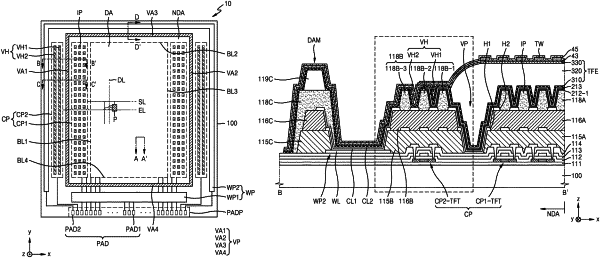
1. A display device comprising:
a substrate comprising a display area and a non-display area;
a circuit portion on the non-display area, the circuit portion comprising a first circuit portion and a second circuit portion;
a valley portion separating the first circuit portion and the second circuit portion from each other; and
a thin film encapsulation layer sealing the display area, the thin film encapsulation layer extending from the display area to the valley portion,
wherein the first circuit portion is between the valley portion and the display area, and the second circuit portion is at an outside of the valley portion and comprises at least one thin film transistor,
an internal layer on the first circuit portion comprises a plurality of grooves extending in each of a first direction and a second direction crossing the first direction, and a plurality of island portions comprising respective upper surfaces that are apart from one another in the first direction and the second direction,
an external layer on the second circuit portion comprises a plurality of grooves extending in the first direction and separated from one another in the second direction, and
the first direction and the second direction are parallel to a main surface of the substrate.
|