| CPC H01L 27/249 (2013.01) [H01L 27/11514 (2013.01); H01L 21/76816 (2013.01); H01L 23/5226 (2013.01); H01L 45/065 (2013.01); H01L 45/085 (2013.01); H01L 45/16 (2013.01); H01L 45/1683 (2013.01)] | 20 Claims |

|
1. A method, comprising:
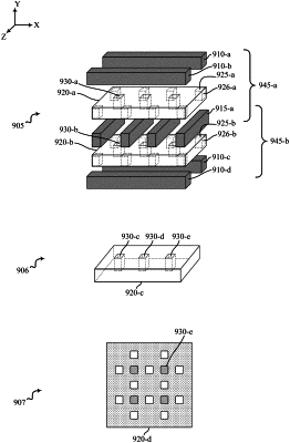
forming pluralities of first vias through a top layer of a stack that comprises a memory material at a memory layer, each plurality of first vias linearly disposed in a first direction;
forming pluralities of second vias through the top layer of the stack, each plurality of second vias linearly disposed in a second direction that is different from the first direction;
forming a plurality of first channels in the memory material, each first channel aligned with a plurality of first vias;
forming a plurality of second channels in the memory material, each second channel intersecting the plurality of first channels; and
filling the plurality of first channels and the plurality of second channels with a dielectric material.
|