| CPC H10B 61/22 (2023.02) [H10B 63/34 (2023.02); H10B 63/845 (2023.02)] | 19 Claims |
|
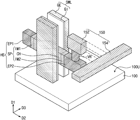
1. A variable resistance memory device, comprising:
a substrate;
horizontal structures spaced apart from each other in a first direction perpendicular to a top surface of the substrate;
variable resistance patterns on the horizontal structures, respectively; and
conductive lines on the variable resistance patterns, respectively,
wherein:
each of the horizontal structures includes a first electrode pattern, a semiconductor pattern, and a second electrode pattern arranged along a second direction parallel to the top surface of the substrate,
each of the variable resistance patterns is between one of the second electrode patterns and a corresponding one of the conductive lines, and
the horizontal structures, the variable resistance patterns, and the conductive lines are sequentially stacked on the top surface of the substrate in the first direction.
|