| CPC H10B 53/30 (2023.02) [H01L 21/0234 (2013.01); H01L 21/02356 (2013.01); H01L 28/60 (2013.01)] | 20 Claims |
|
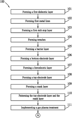
1. A method for manufacturing a ferroelectric memory cell, comprising:
forming a ferroelectric layer which includes a ferroelectric material;
forming a top electrode layer on the ferroelectric layer;
patterning the top electrode layer to form a top electrode;
patterning the ferroelectric layer to form a data storage element;
forming a sidewall spacer aside the top electrode such that the data storage element has a peripheral region beneath the sidewall spacer; and
treating the ferroelectric material using a gas plasma such that the peripheral region of the data storage element has at least 60% of ferroelectric phase, to form the ferroelectric memory cell.
|