| CPC H10B 51/30 (2023.02) [H01L 29/6684 (2013.01); H01L 29/78391 (2014.09)] | 20 Claims |
|
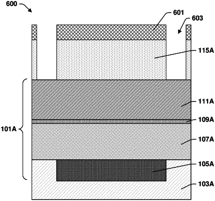
1. A method of forming an integrated circuit device, the method comprising:
forming a ferroelectric layer by an atomic layer deposition (ALD process) using chlorine-free precursors, wherein the ferroelectric layer has a top surface that results from the ALD process and the chlorine-free precursors comprise a hafnium (Hf) compound and a zirconium (Zr) compound;
prior to any further processing of the ferroelectric layer subsequent to the ALD process, depositing either a dielectric layer-metal oxide semiconductor layer stack, a metal oxide semiconductor layer, or a top electrode layer directly over and in contact with the top surface.
|