| CPC H10B 41/30 (2023.02) [H01L 29/40114 (2019.08); H01L 29/42328 (2013.01); H01L 29/66492 (2013.01); H01L 29/66545 (2013.01); H01L 29/66825 (2013.01); H01L 29/7833 (2013.01); H01L 29/7881 (2013.01)] | 14 Claims |
|
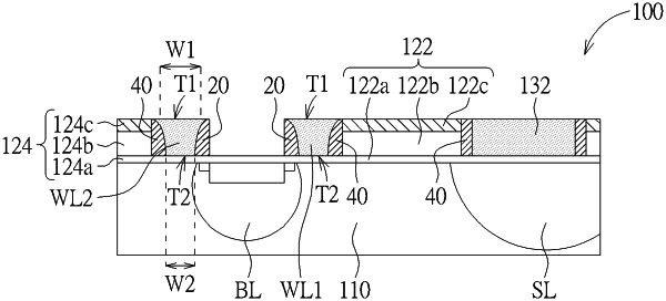
1. An array of programmable memory, comprising:
a first row of floating gate and a second row of floating gate disposed on a substrate along a first direction;
two spacers disposed between and parallel to the first row of floating gate and the second row of floating gate; and
a first row of word line sandwiched by one of the spacers and the adjacent first row of floating gate, and a second row of word line sandwiched by the other one of the spacers and the adjacent second row of floating gate, wherein the first row of word line and the second row of word line both have cross-sectional views broaden from bottom to top.
|