| CPC H10B 12/482 (2023.02) | 15 Claims |
|
1. A method for fabricating a semiconductor device, comprising:
providing a substrate;
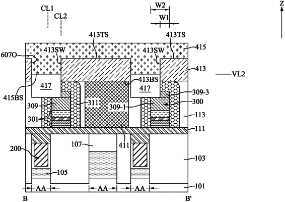
forming a bit line conductive layer on the substrate and a bit line inner capping layer on the bit line conductive layer, wherein the bit line conductive layer and the bit line inner capping layer together configure a bit line structure;
forming a bit line spacer capping layer covering the bit line structure;
forming a cell contact adjacent to the bit line structure;
forming a blanket pad layer on the bit line spacer capping layer and the cell contact;
forming a plurality of pad openings along the blanket pad layer and extending to the bit line spacer capping layer and the bit line inner capping layer to turn the blanket pad layer into a plurality of landing pads, wherein the bit line inner capping layer has a lower portion and an upper portion having a width smaller than a width of the lower portion, wherein a top surface of the upper portion of the bit line inner capping layer is covered by the bit line spacer capping layer, wherein a top surface of the lower portion of the bit line inner capping layer and a side surface of the upper portion of the bit line inner capping layer are exposed within each of the plurality of pad openings; and
selectively forming a sealing layer on the plurality of landing pads and covering upper portions of the plurality of pad openings to form a plurality of air gaps between the bit line conductive layer and the plurality of landing pads, wherein the plurality of air gaps are formed between a bottom surface of the sealing layer and the top surface of the lower portion of the bit line inner capping layer.
|